The Blueprint of Speed: A Deep Dive into High Frequency PCB Technology
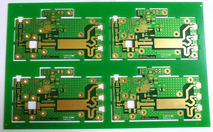
High Frequency PCB used in 5G, aerospace, automotive radar, and high-speed communication systems
In the rapidly evolving landscape of modern electronics, the demand for faster data transmission and higher signal integrity has never been more critical. As we push the boundaries of 5G connectivity, autonomous driving, and advanced aerospace communications, the backbone of these innovations is the high frequency PCB. Unlike standard printed circuit boards, these specialized components are engineered to handle signals in the gigahertz (GHz) range, where the margin for error is practically zero.
Understanding the High Frequency PCB
A high frequency PCB is specifically designed to minimize signal loss and maintain electromagnetic compatibility (EMC) when operating at frequencies typically above 500 MHz. At these elevated speeds, electrical signals behave less like simple currents in a wire and more like electromagnetic waves. This shift in physics requires a fundamental rethink of board materials, layout, and manufacturing tolerances.
In standard FR-4 boards, signal attenuation and dielectric loss become prohibitive at high frequencies. To solve this, high frequency boards utilize specialized substrates—often ceramic-filled or PTFE (Teflon) based—that offer a much lower dissipation factor and a stable dielectric constant.
Core Material Characteristics
When selecting materials for a high frequency PCB, engineers focus on three primary metrics:
- Dielectric Constant ($D_k$): Stability is key. If the $D_k$ fluctuates with temperature or frequency, the phase velocity of the signal changes, leading to distortion. High-end boards aim for a low and consistent $D_k$.
- Dissipation Factor ($D_f$): This measures how much energy is lost as heat within the substrate. A lower $D_f$ ensures that the signal reaches its destination with maximum strength.
- Coefficient of Thermal Expansion (CTE): Because high-frequency components often generate significant heat, the board material must match the thermal expansion of the copper traces to prevent delamination or solder joint failure.
Design Challenges and Best Practices
Designing a high frequency PCB is an exercise in precision. Every millimeter of copper trace acts as an inductor, and every gap acts as a capacitor. If these parasitic elements aren’t managed, the board will suffer from “crosstalk,” “ringing,” and signal reflection.
Controlled Impedance
To prevent signal reflections, the impedance of the traces must be perfectly matched to the source and the load. This involves calculating the exact width of the traces based on the height of the dielectric layer and the properties of the material.
Shielding and Grounding
In high-frequency environments, electromagnetic interference (EMI) is the enemy. Designers utilize solid ground planes and “via stitching” (placing rows of vias along the edges of traces) to create an electromagnetic cage, keeping high-speed signals contained and external noise out.
Minimizing Signal Path Length
The physical distance a signal travels matters. At high frequencies, even a slightly longer trace can introduce a phase shift. Designers prioritize “shortest-path” routing and ensure that differential pairs—two traces carrying equal and opposite signals—are kept exactly the same length to maintain timing.
Key Applications of High Frequency PCBs
Where do these high-performance boards actually live? You’ll find them at the heart of the world’s most sophisticated technology:
- Telecommunications: 5G base stations rely heavily on high frequency PCB technology to manage massive MIMO (Multiple Input Multiple Output) antenna arrays and ultra-wideband data streams.
- Military and Aerospace: Radar systems, satellite communications, and electronic warfare equipment require boards that can operate in the X-band (8–12 GHz) and beyond without degrading.
- Medical Technology: High-resolution imaging systems, such as MRI and CT scanners, use high-frequency signals to process massive amounts of biological data in real-time.
- Automotive Industry: Modern ADAS (Advanced Driver Assistance Systems) use 77 GHz radar sensors for collision avoidance and autonomous navigation, making high-speed PCB design a safety-critical requirement.
The Role of Advanced Substrates
While FR-4 is the “workhorse” of the electronics world, it fails in high-frequency applications because its resin binds moisture and its $D_f$ is too high. This is why a high frequency PCB often incorporates materials from specialized vendors like Rogers, Taconic, or Isola.
These materials are often reinforced with woven glass or ceramic to provide structural integrity while maintaining the electrical “transparency” needed for high-speed waves. For instance, PTFE-based materials are prized for their incredibly low loss, though they are notoriously difficult to manufacture due to their “slippery” nature and soft texture.
Manufacturing Nuances
The fabrication process for a high frequency PCB is significantly more rigorous than that of a standard board. It requires:
- Precision Etching: The width of the copper traces must be controlled within microns to maintain impedance.
- Plasma Desmearing: Because PTFE materials don’t respond well to traditional chemical cleaning, plasma treatment is used to ensure that holes are clean and ready for plating.
- Surface Finishes: Traditional HASL (Hot Air Solder Leveling) creates an uneven surface that is detrimental to high-speed signals. Instead, finishes like ENIG (Electroless Nickel Immersion Gold) or Immersion Silver are preferred for their flatness and conductivity.
Conclusion: Partnering for Success
As the world moves toward 6G, IoT expansion, and sophisticated AI edge computing, the importance of the high frequency PCB will only grow. These boards are no longer just “carriers” for components; they are components themselves, behaving as complex waveguides that dictate the performance of the entire system. Because the tolerances are so tight and the material costs are high, there is no room for trial and error in the production phase.
To ensure your project meets its performance targets without costly redesigns, it is essential to collaborate with an experienced High Frequency PCB Manufacturer. A specialized partner can provide the engineering support, material expertise, and precision fabrication necessary to turn your high-speed designs into a functional reality. Whether you are developing a satellite transponder or a next-gen medical sensor, the right manufacturing expertise is the final piece of the high-frequency puzzle.