The Architecture of Modern Electronics: A Deep Dive into the Multilayer PCB
Multilayer PCB structure illustrating signal layers, power planes, and dielectric insulation
In the early days of electronics, a simple single-sided or double-sided board was sufficient to connect a few transistors and resistors. However, as the world transitioned into the era of smartphones, supercomputers, and high-speed telecommunications, the demand for complexity grew exponentially. Enter the multilayer PCB—the sophisticated, multi-tiered highway system of the electronics world. By stacking layers of conductive material and insulation, this technology has allowed engineers to pack incredible processing power into devices that fit in the palm of a hand.
What Defines a Multilayer PCB?
A multilayer PCB is a printed circuit board that consists of three or more conductive copper layers. These layers are separated by insulating materials (typically prepreg and core layers) and are bonded together under high pressure and temperature to form a single, cohesive unit. While a 4-layer or 6-layer board is common for consumer electronics, advanced industrial applications can utilize boards with 30 layers or more.
The primary goal of a multilayer PCB is to increase the available area for wiring while minimizing the physical footprint of the device. By moving traces from the surface into internal layers, designers can achieve a level of circuit density that is physically impossible on simpler boards.
The Anatomy of the Stack-Up
To understand how a multilayer PCB functions, one must visualize its internal “sandwich” structure. It isn’t just a stack of copper; it is a carefully engineered sequence of materials:
- Top and Bottom Layers: These are the visible layers where components are typically soldered.
- Internal Signal Layers: These “hidden” layers carry the bulk of the electrical signals between components.
- Plane Layers (Power and Ground): In a multilayer PCB, entire layers are often dedicated to power distribution and grounding. This helps stabilize voltages and reduces electromagnetic interference (EMI).
- The Dielectric (Prepreg and Core): These insulating layers keep the copper signals from touching each other, acting as the structural “glue” of the board.
Why the Multilayer PCB is Essential
The transition from double-sided boards to a multilayer PCB architecture offers several transformative advantages for modern hardware:
1. Increased Circuit Density
By utilizing internal layers, designers can route thousands of connections in a very small space. This is the primary reason why modern laptops and medical devices can be so thin while remaining incredibly powerful.
2. Reduced Electromagnetic Interference (EMI)
One of the greatest challenges in high-speed design is “noise.” A multilayer PCB allows designers to place signal layers between ground or power planes. This configuration acts as a shield, containing electromagnetic waves and preventing them from interfering with other parts of the circuit.
3. Lower Weight and Smaller Size
Because a multilayer PCB consolidates multiple functions into a single board, it eliminates the need for bulky connectors and multiple separate boards. This reduction in hardware translates directly to lighter, more portable products.
4. Improved Signal Integrity
At high frequencies, the distance a signal travels and the environment it travels through are critical. Multilayer boards allow for controlled impedance and shorter trace lengths, ensuring that data moves at maximum speed without corruption.
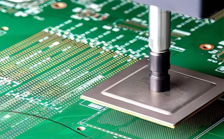
The Complex Manufacturing Process
Creating a multilayer PCB is significantly more demanding than producing basic boards. It requires a high degree of precision and specialized equipment:
- Lamination: The various layers must be perfectly aligned. Even a microscopic misalignment during the pressing process can result in a “dead” board where vias (vertical holes) fail to connect to the correct internal traces.
- Via Technology: Since layers are stacked, connections between them are made through “vias.” In advanced boards, these include blind vias (visible on one surface but not the other) and buried vias (hidden entirely within the internal layers), which maximize routing space.
- Drilling and Plating: High-speed laser drilling is often used to create the tiny holes required for high-density interconnects, followed by a copper plating process to ensure electrical continuity throughout the stack.
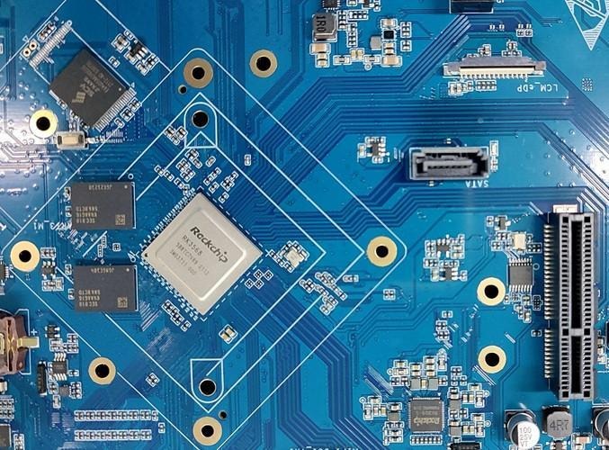
Common Applications
The multilayer PCB is the heart of almost every advanced electronic system today:
- Computers and Servers: From the motherboard in your PC to the massive arrays in data centers.
- Telecommunications: 5G equipment and fiber optic interfaces rely on multilayer stacks to handle immense data throughput.
- Medical Equipment: Portability in ultrasound machines and heart monitors is made possible by high-density multilayer designs.
- Aerospace: Space-constrained environments like satellites and jet cockpits require the reliability and compactness of these boards.
Conclusion: Partnering with Precision
As technology continues to shrink, the complexity of the multilayer PCB will only increase. Designing these boards is an art form that balances electrical physics with mechanical constraints. However, a brilliant design is only as good as its execution. Because the internal layers are permanent once laminated, any defect during the manufacturing stage can lead to the failure of the entire assembly.
To bring your complex designs to life without the risk of delamination or signal failure, it is crucial to select a world-class Multilayer PCB Manufacturer. A partner with advanced lamination technology and rigorous automated optical inspection (AOI) can ensure that every internal connection—no matter how many layers deep—is perfect. Whether you are scaling a consumer gadget or building an industrial control system, the right manufacturing expertise is the key to a reliable, high-performance product.